

Fast and Precise Inspection from Above and Below

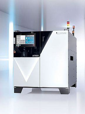
iS6059 Double-Sided Inspection – innovative quality control of PCBA top and bottom sides
With innovative 3D camera technology, the iS6059 Double-Sided Inspection 3D-AOI system inspects THT components, THT solder joints, press-fit and SMD components shadow-free and at high precision on the upperside and underside of the printed circuit board. The products are inspected at high speed in 2D, 2½D and 3D. As a result, the iS6059 Double-Sided Inspection stands for maximum defect detection and highest throughput. Different lighting can be used flexibly and so provide inspection results in excellent quality.


Inspection scope


- A convincing concept: two powerful 3D XM sensor modules for simultaneous quality inspection from above and from below
- First-rate inspection quality: Shadow-free inspection thanks to 2x8 angled cameras
- System flexibility: reliable handling of a wide range of different inspection objects
- Verified zero defect slippage thanks to integrated verification
- Minimal time and training requirements thanks to Viscom standard software
- Reduction of cycle times thanks to inspection from both sides
- Global libraries, global calibration: Transferability to all systems
- Outstanding inspection program optimization thanks to flexible single and multiline verification solutions
- Simple operation and inspection program generation with vVision
- High-performance OCR software
- Connection via horizontal interfaces along the production line
- Viscom Quality Uplink: intelligent networking of Viscom inspection systems along the production line
- Production line control and product traceability
- Connection to vertical interfaces for communication with MES systems
- Statistical process control with Viscom SPC/vSPC
- Offline programming stations for increased efficiency
- Optional connection to the digital multi-purpose platform vConnect
Components: THT, press-fit and SMD
| Solder joints: 3D inspection of PCB upper and bottom sides after reflow, wave or selective soldering |
| Defects/characteristics: |
| SMD: Presence, XY position, rotation, component height, polarity, missing solder, soldering defects, lifted heads/tombstoning, bridging |
| THT: Presence, XY position, missing solder, soldering defects, bridging, pin height, non-wetting on pins, non-wetting on pads |
| Optional: Free area analysis, wobble circle error, color ring analysis, OCR, blow holes in the solder joint, solder ball/solder sputter |
| DIMENSIONS | |
| System housing: | 1100 mm x 1756 mm x 1753 mm (W x D x H) |
| CAMERA TECHNOLOGY | |
| 3D sensor technology: | 2 x XMu-II |
| Z-resolution: | 0.5 µm |
| Z-range: | Up to 30 mm (1.2") |
| Angled view cameras | |
| Number of megapixel cameras: | 8 |
| Orthogonal camera | |
| Resolution: | 13 µm |
| Field of view: | 50 mm x 50 mm (2" x 2") |
| INSPECTION SPEED | Up to 100 cm²/s (both sides combined) |
| HANDLING | |
| PCB dimensions: | 508 mm x 560 mm (20" x 22"); |
| SOFTWARE | |
| User interface: | Viscom vVision |
| Statistical process control: | Viscom vSPC/SPC, open interface (optional) |
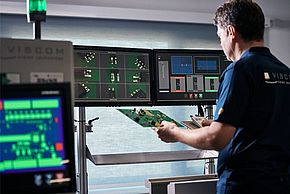
| Verification station: | Viscom vVerify |
| Remote diagnosis: | Viscom SRC (optional) |
| Programming station: | Viscom PST34 (optional) |
ADVANTAGES AT A GLANCE
- Maximum defect detection on both sides
- Flexible handling options
- Unmatched 3D camera technology
- Different illuminations
- Complete process tracking


